 -Welcom to Okenshoji Co., Ltd HomePage
for Electron Microscopy--Welcom to Okenshoji Co., Ltd HomePage
for Electron Microscopy-
-Welcom to Okenshoji Co., Ltd HomePage
for Electron Microscopy--Welcom to Okenshoji Co., Ltd HomePage
for Electron Microscopy-![]()
Ever since the company was founded in 1950, our primany concern business is the supply of quality accessories for Electron and Light Microscopy like following Micro Grid(Lacy Carbon Film), Collodion・Formvar Substrate, Elastic Carbon Substrate, High Resolution Carbon Substrate, Electrically Conductive Double Sided Carbon Tape and so on so forth.
For customers ordering from outside Japan.
Woomyoung Incorporation
Daecheongtower#434, 623 Gaepo-ro, Gangnam-Gu, Seoul, KOREA
TEL:82(2)3412-6999 FAX:82(2)3412-6009
E-mail:woomyoung@daum.net
All other countries:
Okenshoji Co., Ltd
Kawakami Building 3F
5-3-11, Soto-Kanda, Chiyoda-Ku
Tokyo 101-0021
JAPAN
TEL:81(3)5826-8642 FAX:81(3)5826-8643
E-mail: info@okenshoji.co.jp
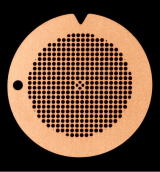
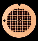
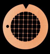
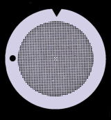
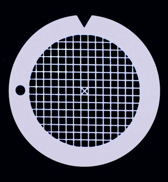
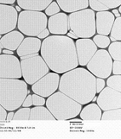
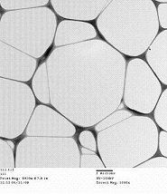
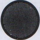
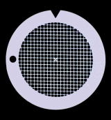
Code#10 Grid with Support Film for TEM It is requested for Support Films that they prevent specimen from electron beam thermal affect, damage and minimize broken part of grid square. We provide various kinds of Micro Grids, Micro Grids with Plastic Film and Carbon Film as below. Please select the suitable one for your research work considering specimen, accelerating voltage and magnification, etc. We also providing many kinds of Grids other than below. It is welcome to consult with us when you cannot find a suitable one.
STEM Cu100P Grid STEM Cu150P Grid STEM Cu 300P Grid 250 mesh fit. 25μthickness 167 mesh. 30μthickness 83 mesh fit. 15μ thickness STEM Mo50P Grid STEM Mo100P Grid STEM Mo150P Grid 500 mesh fit. 10μ thickness 250 mesh fit. 10μ thickness 167 mesh fit. 10μ thickness
#10-1001 Micro Grid NS-C15 (Based on Cu 150P equivalent to 170 mesh grid, Lacy Carbon film) 25 pcs per box.Opening ratio more than 60%, wide effective observation area obtained. Hole diameter around 1.5 to 8 μm. Easy to ovserve acicular shape of specimen. Suitable for ultra-high resolution observation of acicular, fabric and plate shape of thin specimen. Wide opening and adequate thickness of carbon enable to bring deterioration of contrast even at the place of flame crossing. Magnification: Low to hundreds of thousands.
STEM Cu150P Grid
#10-1026 Micro Grid NS-M15 (based on Mo150P, equivalent to 170 mesh grid) 25pcs per box.More than 60% open ratio typical lacy structure Micro Grid. Micro Grid size around 2 to 7μm. Carbon film thickness is around 10 to 15nm. Since this one is Mo Grid, suitable for elemental analysis, too.
STEM Mo150P Grid
#10-1002 Micro Grid NP-C15 (based on Cu 150P equivalent to 170 mesh grid, Holey Carbon Film) 25 pcs per box.Less than 60% open ratio holey structure Micro Grid. Hole diameter around 1.0 to 9μm. Suitable for high resolution observation of plate shape specimen. Also can be used as the calibration sample of beam alignment. Open ratio is not as good as NS-C15 but must be economical when samples have large observation area. Magnification: Several to hundreds of thousands.
STEM Cu 150P Grid
#10-1027 Micro Grid NAP-M15 (based on Mo150P) 25pcs per box.Opening ratio 60% or less lacy carbon grid. Micro Grid size around 1 to 8μm. Carbon film supported. Since this one is Mo Grid, suitable for elemental analysis.
STEM Mo150P Grid
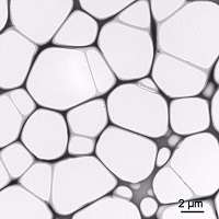
#10-1003 Micro Grid RO-C15 (based on Cu150P, Lacy Carbon Film) 25pcs. per box.Has the net shape mesh structure and 70% or better open ratio typical lacy structure Micro Grid. Micro Grid size around 3 to 8μ. Carbon coating is around 70nm so this has good resistance to organic solvent and able to realize less specimen drift. Has temperature resitance up to 500℃ in vacuum condition.
STEM Cu150P Grid
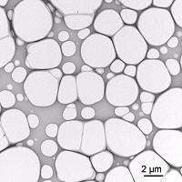
#10-1004 Micro Grid RT-M10 (based on Mo100P, Lacy Carbon Film) 25 pcs per box.Has the net shape mesh structure and 70% or better open ratio typical lacy structure Micro Grid. Micro Grid size around 3 to 8μ. In order to obtain much better temperature resistance, it is supported by Mo100P, so that able to heat samples up to around 1,000℃ in vacuum condition. Carbon coating is around 70nm so this has good resitance to organic solovent and to realize less specimen drift.
STEM Mo100P Grid
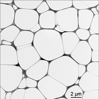
#10-1016 Micro Grid NH-C15 (based on Cu150P) High opening ratio Micro Grid. 25 pcs per box.Better to use more than 200K magnification. Opening ratio 80% or better lacy carbon grid. Hole diameter around 1 to 8 μm. 10-15nm Carbon film supported. Suitable for plate shape thin specimen, materials slices, long acicular shape specimen, acicular crystals and fine grain.
#10-1017 Micro Grid NL-C30 (based on Cu300P) Large opening Micro Grid 25 pcs per box.Magnification up to 400K. Opening ratio 80% or better. Hole diameter 10-15μm. Carbon coating around 10nm-15nm. Suitable for materials slices, biological slices, plate shape thin specimen, long acicular shape specimen and acicular crystals.
Plastic Substrate with Carbon
Suitable for the use of magnification from several to ×30,000. Good for observation of article shape materials, thin film specimen. Each Plastic Substrate is supported by evaoplated thin layer of Carbon (Thickness 10-15nm).
#10-1006 Collodion Film COL-C15 (based on Cu150P) 25 pcs per box.Widely accepted Nitorocellulose films for TEM observation (30-40nm thickness) supported by Carbon layer (10-15nm thickness) on Cu150P grid. Suitable to use 75-200kV TEM.
#10-1028 Collodion Film COL-M15 (based on Mo150P) 25 pcs per box.Widely accepted Nitorocellulose films for TEM observation (30-40nm thickness) supported by Carbon layer (10-15nm thickness). Since this is based on Mo150P grid, good to use for elemental analysis, and suitable to use for 75-200kV TEM..
#10-1007 Collodion Film COL-C10 (based on Cu 100P) 25 pcs per box.
Widely accepted Nitorocellulose films for TEM observation (30-40nm thickness) supported by Carbon layer (10-15nm thickness). Since this is based on Cu100P grid, this is able to realize less specimen drift than COL-C15. Suitable to use for 75-200kV TEM.
#10-9999 Collodion Film COL-M10 (based on Mo100P) 25 pcs per box.
Also available this type.
#10-1008 Formvar Film PVF-C15 (based on Cu150P) 25pcs per box.
Widely accepted Polyvinyl formal(Formvar) films for TEM observation (30-40nm thickness) supported by Carbon layer(10-15nm thickness) on Cu150P grid. Suitable to use for 75-200kV TEM.
#10-9999 Formvar Film PVF-M15 (based on Mo150P) 25 pcs per box.Also available this type.
#10-1009 Formvar Film PVF-C10 (based on Cu100P) 25 pcs per box.
Widespread Polyvinyl formal(Formvar) films for TEM observation (30-40nm thickness) supported by Carbon layer (10-15nm thickness). Since this is based on Cu100P grid, enable to realize less specimen drift than Cu150P. Suitable to use for 75-200kV TEM.
#10-9999 Formvar Film PVF-M10 (based on Mo100P) pcs per box.
Also available this type.
Carbon Substrate
Carbon substrate has better resistance against Electron beam exposure and Orgnic solvent suspension specimen when observation with 100kv or more. Stable substrate against Electron beam exposre, drift and Orgnic solvent suspension specimen. Please choose the suitable one according to each feature of film.
#10-1012 Elastic Carbon Film ELS-C10 (based on Cu100P) 25 pcs per box.
This has better beam transparency than plastic substrate so suitable to use for high magnification research work. Most stabel substrate against Flectron beam exposure, drift and Orgnic solvent suspenshion specimen with 100kV or more obserbation. Magnification up to around ×100kV. Specimen are fine powders, plate shape ones, acicular shape ones and fibrous type. High polymer base material has 15-20nm thickensss and Carbon film thickness has 20-25nm. This structure enable not bo be dissolved with ehyl acetate, isoamyl acetate, ethyl alcohol, butyl alcohol, aceton, cyclohexane and so on. However, the base film thickenss is very thin, there might come unforseen influence to specimen due to many factors of Organic solvent permeability, expansion and surface tention after drying and so on. So, it is recommended to confirm if any influence is available after drying specimen.
#10-1030 Elastic Carbon Film ELS-M10(based on Mo100P) 25pcs. per box.
This is also well-known and widespread film Triacetylcellulose film(20-30nm)supported by Carbon layker(10-15nm thickness) against electron beam exposure. For 100-300kV TEM.
#10-1013 High-Resolution Carbon Film HRC-C10(based on Cu100P) 25pcs. per box.
This is for high magnification research work because Carbon film thickenss 15nm or under and Micro Grid are united. So, the structure brings better resistance to electron beam exposure and realizes less drift. Target magnification is around x300k. The best suited for fine powders, plate shape ones, acicular shape ones and fibrous type specimen. About 0.5% of Fe, Si, Cl and so on are included due to using Carbon for High-Resolution observation.
#10-1031 High-Resolution Carbon Film HRC-M10(based on Mo100P) 25pce. per box.
This is for high magnification research work Because Caron film thickenss 15nm or under and Micro Grid are united. So, the strucute brings better resistance to electron beam exposre and realizes less drift. Direct magnificication is up to x600K.
#10-1014 Ultra High-Resolution Carbon Film UHR-C10(based ib Cu100P) 25pcs. per box.
This is for high magnification research work because Carbon film thickness 10nm or under and Micro Grid are united. So, the structure brings better resistance to electron beam exposure and realizes less drift. Target magnificicatin is x300K or over. The best suited for fine powders, plate shape ones, acicular shape ones and fibrous type specimen. About 1.0% of Fe. Si, Cl and so on are included due to using Carbon for Ultra High-Resolution observation.
#10-1032 Ultra High-Resolution Carbon Film UHR-M10(based on Mo100P) 25pcs. per box.
This is high magnification research work because Carbon film thickness 10nm or under and Micro Grid are united. So, the structre brings better resistance to electron beam exposure and realizes less drift. Direct magnification is up to around x800K. For 100-300kV TEM.
#10-1015 Super High-Resolution Carbon Film SHR-C075(based on Cu075P) 25pcs. per bos.
This is for high magnification research work because Carbon film thickenss 6nm or under united with Micro Grid. The thinnest Carbon film thickness enable higher resolution research work than the above threee mentioned films. About 1.0% of Fe. Si, Cl and so on are included due to using Carbon for Super High-Resolution observation. When using, please take care of electron beam intensity.
#10-1022 Carbon Film C10-M05(based on Mo50P) 10pcs. per box.
Using high-purity Carbon to form film thickness around 8-13nm. Since using high-purity Carbon, this film is ideal for elemental analysis. This also has better resistance to electron beam exposure and realizes less drift, in addition stalbe against every Organic solvent. Possible to heat specimen up to around 1000℃ in vacuum condition. for 75-300kV TEM.
#10-1023 Carbon Film C20-C10 (based on Cu100P) 10pcs. per box.
Using high-purity Carbon to form film thikness around 15-20nm. This is also has better resistance to electron beam exposure and realizes less drift, in addtion, stable against every Organic solivent. Possible to heat sepcimen up to around 500℃ in vacuum condtion. For 75-300kV TEM.
#10-1024 Germanium Film G20-M05) (based on Mo50P) 10pcs. per box.
Using high-purity Germanium to form film thikness around 8-13nm. This also has better resistance to electron beam exposure and realizes less drift, in addition stable against every Organic solvent. Using high-purity Germanium enable to do elemental analysis. Possible to heat specimen up to around 700℃ in vacuum condition. For 75-300kV TEM.
#10-1025 Gerumanium Film G20-C10 (based on Cu100P) 10pcs. per box.
Using high-purity Germanium to form film thikness around 15-20nm. Since using high-purity Gemanium this film is ideal for elemental analysis. This slso has better resistance to electron beam exposre and realizes less drift, in addtion, stable against every Organic solvent. Possible to heat specimen up to around 500℃ in vacuum condition. For 75-300kV TEM.
#10-1037 Clear film MMA-C15 (based on Cu150P) 25pcs. per box.
Acrylic thin film(Thikness around 30-40nm) with Carbon supported by 10-15nm. Clear film has lower density and less spotted than collodion film or Formvar Film. This feature brings clear TEM images with better contrast. For 75-200kV TEM.
#10-1038 Clear Film MMA-C10 (based on Cu100P) 25pcs. per box.
Acrylic thin film(Thikness around 30-40nm) with Carbon supported by 10-15nm. Clear Film has lower density and less spotted than Collodion Film or Formvar Film. This feature brings clear TEM images with better contrast. MMA-C10 has less image drift than MMA-C15, suitable for higher magnification ovservation. For 75-200kV TEM.
#10-1039 Clear Film MMA-M15 (based on Mo150P) 25pcs. per box.
Acrylic thin film (Thikness around 30-40nm) with Carbon supported by 10-15nm. Clear Film has lower density and less spotted than Collodion Film or Formvar Film. This feature brings clear TEM images with better contrast. Suitable for elemental analysis. For 75-200kV TEM.
#10-1040 Clear Film MMA-M10 (based on Mo100P) 25pcs. per box.
Acrylic thin film (Thikness around 30-40nm) with Carbon supported by 10-15nm. Clear Film has lower density and less spotted than Collodion Film or Formvar Film. This feature brings clear TEM images with better contrast. MMA-M10 has less image drift than MMA-M15, suitable for higher magnification overvation. Suitable for elemental analysis. For 75-200kV TEM.
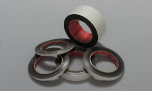
Electrically Conductive Double Sided Carbon Tape (Aluminum Base)
Alminium base substrate brings smoother surface of the tape. So when with lower or midium magnification, operators no need to take care of the background. This alminium substrare is a new technology and improve the quality like less drift, enable to observe fine particles with high magnification. Surface of the tape is conductive adhesive and contains Carbon powder as electrically conductive filler.
#15-1095 Electrically Conductive Double Sided Carbon Tape(Alminum Base) 5mm wide x 20m long
#15-1096 Electrically Conductive Double Sided Carbon Tape(Alminum Base) 8mm wide x 20m long
#15-1097 Electrically Conductive Double Sided Carbon Tape(Alminum Base) 10mm wide x 20m long
#15-1098 Electrically Conductive Double Sided Carbon Tape(Alminum Base) 12mm wide x 20m long
#15-1099 Electrically Conductive Double Sided Carbon Tape(Alminum Base) 20mm wide x 20m long
#15-1100 Electrically Conductive Double Sided Carbon Tape(Alminum Base) 50mm wide x 20m long